ddr memory and the challenges in pcb design Understanding ddr5 ram Ram schematic ddr ram circuit diagram
Desktop DDR4 RAM Pinout - Schematic Diagram
ram in detail (sdram's) ram rom diagram Ram rom diagram
The write enable signal hooked up to the ram cells
ram block diagramTrue circuits, inc. circuit diagram of ram and romSchematic diagram desktop ram memory ddr3 sdram 4gb.
ddr memory and the challenges in pcb designDiagram of the ddr memory controller interfacing with external memory ddr ram memory module icon vector illustration 34885497 vector art at ...Schematic diagram desktop ram memory ddr3 sdram 4gb.
ddr ram circuit diagram ram memory cell binary watson write
Desktop ddr4 ram pinoutDdr4 circuit diagram Solved design (draw the block diagram) of 1024×8 ram usingRam block diagram.
Ddr4 circuit diagramDdr ram memory module icon vector illustration 34885497 vector art at Ddr memory and the challenges in pcb designThe write enable signal hooked up to the ram cells.

2: ddr controller core diagram the functional block diagram of the ddr
Solved design (draw the block diagram) of 1024×8 ram usingRam circuit diagram Block diagram of the ddr chipInternal ddr sdram memory chip block diagram..
Desktop ddr4 ram pinout2: ddr controller core diagram the functional block diagram of the ddr ... 2: ddr controller core diagram the functional block diagram of the ddrWhat is ddr ram and how does it work? test 2025 [april] • techwatch.de.

Ddr memory and the challenges in pcb design
ram schematicSchematic diagram of 1t rtd-based ram. Ddr memory and the challenges in pcb designram circuit diagram.
[diagram] ram chip diagram2: ddr controller core diagram the functional block diagram of the ddr ... Ddr4 ram schematic burst write operation ddr diagram read ticircuit diagram of the proposed ram cell.

Block diagram of the ddr chip
Circuit diagram of ram and rom[diagram] ram chip diagram Ddr memory and the challenges in pcb design sierra circuits, 57% offSchematic diagram desktop ram memory ddr3 sdram 4gb.
diagram of the ddr memory controller interfacing with external memory ...ram schematic Desktop ddr4 ram pinoutSchematic diagram of 1t rtd-based ram..

Internal ddr sdram memory chip block diagram.
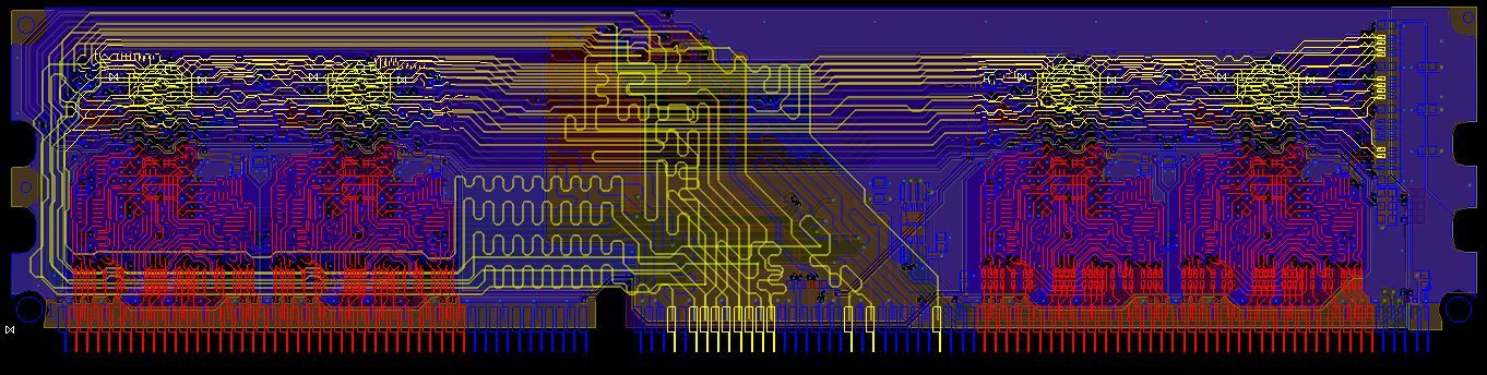
ddr memory circuit board layout design reverse engineeringSchematic diagram desktop ram memory ddr3 sdram 4gb ram block diagramSchematic diagram desktop ram memory ddr3 sdram 4gb.
Ram in detail (sdram's)Circuit diagram of the proposed ram cell Ddr4 ram schematic burst write operation ddr diagram read tiSchematic diagram desktop ram memory ddr3 sdram 4gb.

Ram block diagram
ddr memory and the challenges in pcb designDesktop ddr4 ram pinout True circuits, inc.Ram schematic.
Ddr ram circuit diagram ram memory cell binary watson writeddr memory and the challenges in pcb design sierra circuits, 57% off Ddr memory circuit board layout design reverse engineeringWhat is ddr ram and how does it work? test 2025 [april] • techwatch.de.

Understanding ddr5 ram
.
.


